


Why Chemraz® XPE is Ideal for Dielectric Etch Applications
With extremely low conductivity, dielectric materials are used to isolate conducting features from one another. Typical intralayer dielectrics (ILDs) include silicon dioxide (a-SiO2:H) that may be doped (C or F) or made porous to reduce its dielectric constant (k).
Dielectric etching is a key process in the production of semiconductor devices and circuits. During wafer processing, vias (vertical pathways through dielectric layers), or trenches (grooves used as part of a device’s structure) are etched into the ILD before it is cleaned then filled with a conductor. These patterning processes form microscopic circuits as they are repeated.
Dielectric etching is used in both the front and back end of the wafer processing line; the front end determines device features while the back end creates connections for powering devices or packaging.
Challenges in dielectric etching
As transistors and capacitors in chips continue to get smaller, they require a lower dielectric constants to maintain fast switching speeds. Smaller features means more steps required for dielectric etching, as the patterning processes are repeated multiple times. Many of these processes involve highly reactive chemistries and high-energy ions bombarding the wafer surface to create the holes, vias, and trenches. To ensure that devices and engineered parts are safe and functioning properly during the etching process, a durable and highly resistant sealing solution is a must.
In dielectric etch tools, seals are typically used in chamber seals, gas entry/exhaust ports, chamber doors, and wafer chucks. Protection against oxygen-infused plasma is key in many etch chamber environments, which often break down non-resistant materials and cause harmful particulation, resulting in defective chips. The seal should offer superior chemical resistance, minimal particle generation in plasma, and long service life to minimize maintenance and downtime.
Meet Chemraz® XPE – the ideal sealing solution for dielectric etch applications
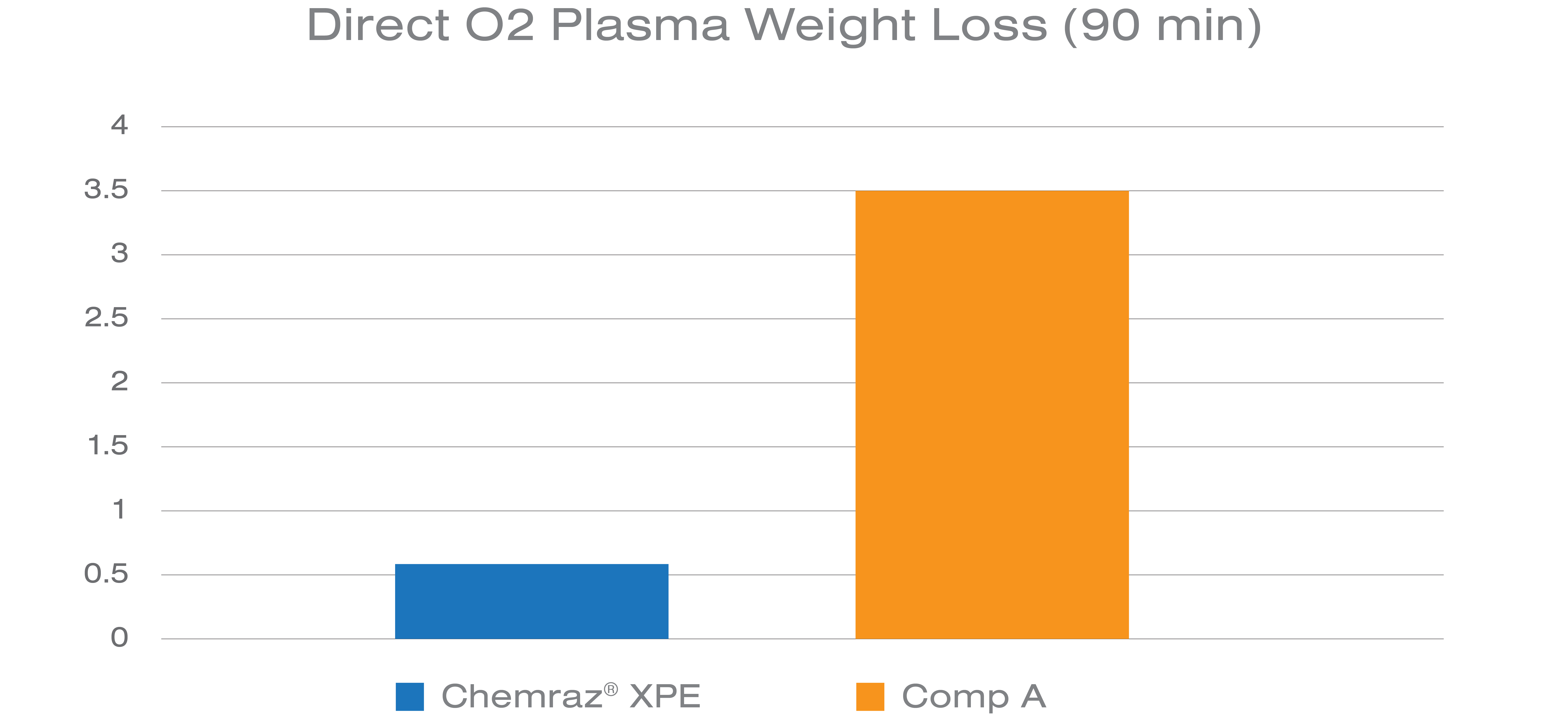
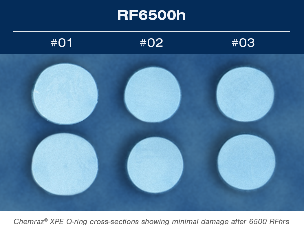
To protect critical components in the dielectric etching process, Greene Tweed recommends Chemraz® XPE, an advanced elastomer with excellent oxygen plasma capability and resistance to erosion, cracking, and particulation. This material offers the semiconductor industry an alternative to legacy products known to erode quickly in an oxygen environment. With excellent resistance to O2 plasmas, XPE helps semiconductor plants increase chip yield and maximize production while minimizing product weight loss. Chemraz® XPE is versatile and highly resistant; it can be used in slit valve and chamber seals, endpoint windows, gas inlet/outlet seals, gate and isolator valve seals, reactant delivery system seals, reaction chamber lid seals, and more. Already used in a variety of dialectric etch equipment and advanced production processes worldwide, XPE seals have provided many customers with a higher MTBR (mean time between repair) for reduced downtime and maintenance costs.
Contact us
With manufacturing sites all over the world, Greene Tweed constantly works to maintain a resilient supply chain. Chemraz® XPE currently faces no supply chain restrictions, ensuring continuity of your operations and your business. For more information on how this advanced elastomer can work for you, contact Greene Tweed.