



How Silicon Photonics and Co-Packaged Optics Are Reshaping AI Infrastructure
Advancements in logic and memory architectures have helped AI become a household name, but the next scaling constraint is increasingly clear: data must move faster, farther, and more efficiently to support agentic, physical, and high-performance AI applications. This bottleneck is now reshaping how semiconductors are designed, fabricated, packaged, and interconnected, adding significant challenges to the manufacturing process and placing new demands on the equipment and its components.

Copper: Step aside, please. Make way for photons
Electrical interconnects with copper for chip-to-chip communications have long been the status quo. But they are increasingly constrained by bandwidth ceilings, and signal integrity limitations – and are a key consumer of precious energy.
This is where silicon photonics and co-packaged optics (CPO) come in. By shifting data transmission from electricity to light, these technologies address one of AI infrastructure’s most urgent commercial challenges: moving more data with less power, lower latency, and greater scalability.
How Silicon Photonics and CPO Help
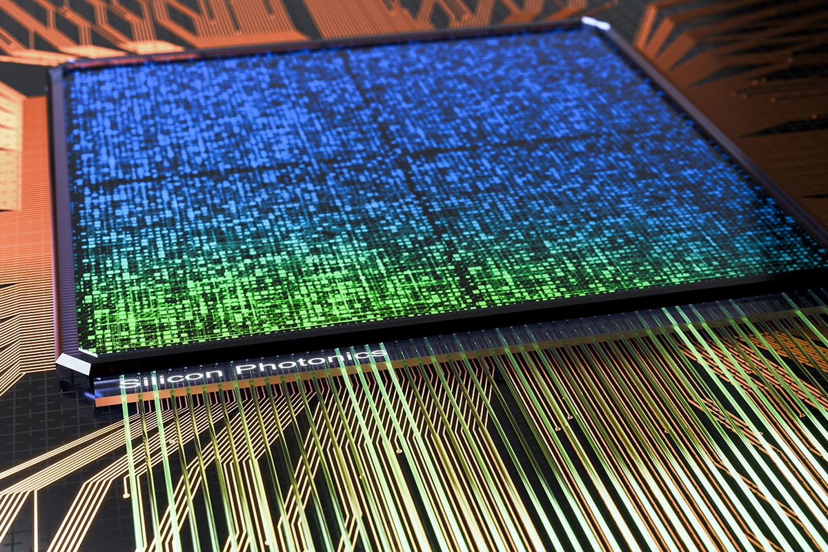
Silicon photonics brings optical engines and photonic integrated circuits, or PICs, closer to application-specific integrated circuits, or ASICs, such as those used in data center network switches.
The shift from electrons to photons brings many benefits:
- Higher bandwidth: Optical links can carry much more data than copper interconnects. For example, CPO platforms such as those from Nvidia and Broadcom can scale network capacity nearly 8x in terms of Tbps (Terabits per second) depending on configuration
- Lower power consumption: Photonics reduces energy loss over distance
- Faster data transfer due to reduced latency
- Better thermal management
In a nutshell, CPO moves optical engines closer to compute by integrating them alongside or within chip packages. This reduces reliance on copper interconnects and helps data move faster and more efficiently.
Why CPO matters now
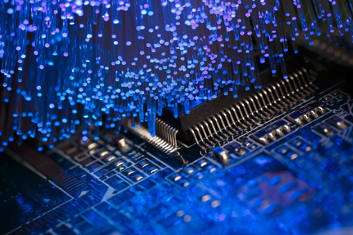
The de facto state-of-the-art in the data center today is pluggable optical modules placed at the edge of a system. Now CPO brings optics directly adjacent to switch ASICs, reducing the distance data must travel electrically and improving the scalability of AI workloads.
And these benefits are needed to support ongoing proliferation of AI in all its forms. Traditional architectures simply can’t keep pace.
Major semiconductor and cloud companies are investing heavily in silicon photonics and CPO, moving from research and niche deployments and, next, toward scaled manufacturing. This investment is broad-based across semiconductor fabs, network switch manufacturers, cloud providers, and semiconductor equipment manufacturers. The performance gains are becoming too significant to ignore, and the market is moving fast. In fact, according to a recent report by IDTechEx, the CPO market alone will grow at a 37% CAGR to USD $20B from 2026 to 2036.
Supporting manufacturing
Silicon photonics manufacturing spans front-end and back-end processes, including etch, deposition, wet processing, hybrid bonding, and advanced packaging integration, with emerging approaches such as glass substrates and panel-level processing adding further complexity.
As these architectures scale, material performance, contamination control, sealing reliability, and thermal stability become increasingly important.

Enter Greene Tweed – Our Role in Enabling this Inflection
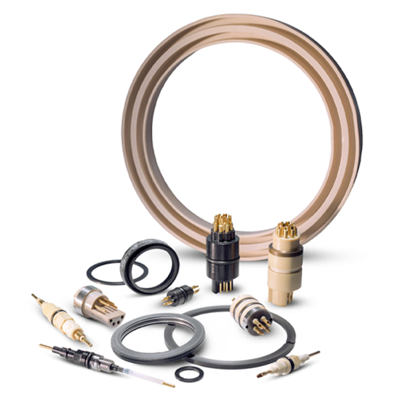
These requirements create a materials challenge as much as a device-architecture challenge. Components used in CPO and silicon photonics manufacturing must support tighter process windows while protecting optical performance across demanding operating environments. Greene Tweed’s portfolio of high-performance polymer sealing solutions and composites is uniquely suited for the demands of silicon photonics and CPO manufacturing. These materials offer:
- Exceptional thermal stability under extreme operating conditions
- Low outgassing properties to protect sensitive optical components
- Chemical resistance for long-term reliability
Greene Tweed excels in technical collaboration during the early design phase. One example of this expertise in action is our design and material work on edge exclusion sealing solutions for electroplating and electrochemical deposition. Collaborating with major equipment providers, we have applied our design and material expertise to develop highly optimized sealing solutions that allow effective part cleaning and resist plate-up on seal surfaces. This work has helped mitigate production issues in the rapidly growing areas of advanced packaging and front-end manufacturing, demonstrating our ability to solve complex, real-world challenges at the intersection of materials science and semiconductor innovation.
For Greene Tweed, this evolution is both a technology shift and a commercial inflection point: advanced materials, precision sealing, and collaborative engineering will be essential to helping customers scale next-generation semiconductor performance.
Bring Us Your Challenges:
If you are exploring silicon photonics, CPO, or next-generation advanced packaging challenges, Greene Tweed is ready to help solve issues in scaling, reliability, manufacturability, and advanced packaging readiness. Contact our team today to learn how our materials and engineering expertise can support your innovation roadmap and help bring your designs from concept to reality.