


Advanced Packaging is HOT!
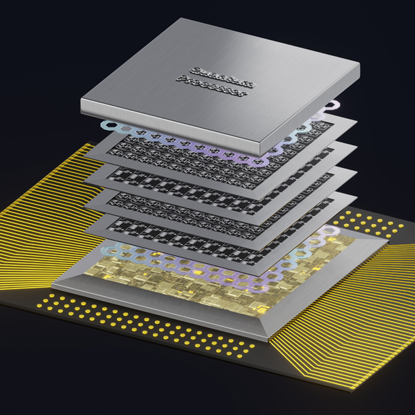
Advanced packaging is one of the most important advancements and a critical part of chip integration, specifically heterogeneous integration. It functions as a bridge between design and manufacturing, allowing multiple chips or chiplets (logic, memory, analog) to be combined into a single, high-performance package. Advanced packaging is set for high growth as the 3D extension of Moore’s Law.
Sealing Challenges in Advanced Packaging
But what new demands does advanced packaging bring to the manufacturing floor? From a sealing and chamber component perspective, Greene Tweed engineers see many of the same issues they already solve across key processes such as etch, deposition, clean, CMP, and others. However, advanced packaging amplifies many sealing issues due to several factors, including new materials being introduced, new temperature tolerances, and different gas chemistries. This requires solutions to address challenges such as particulation due to leaking, seal outgassing, temperature performance, wear caused by new aggressive chemistries, and ongoing needs for extreme cleanliness. The list goes on.
Cutting Contamination and Downtime
Addressing these complexities aligns with Greene Tweed’s expertise in supporting semiconductor equipment and fab customers. By providing solutions for advanced packaging processes, including specialized seal designs for electrochemical etch and deposition, Greene Tweed helps mitigate critical industry hurdles. These innovations in material science and seal design help to reduce chamber contamination, equipment downtime, and the meantime between seal replacement. This, in turn, helps improve overall yields and ensures smooth operations.
What’s Here and What’s Around the Corner?
As a provider of “When it Can’t Fail” sealing and component solutions, Greene Tweed closely monitors the developments in advanced packaging technologies. We collaborate with our customers on their emerging sealing needs related to changing process chemistries, variations in temperature, vacuum needs, and more. One such example is our customer collaboration on unique Edge Exclusion Seals for electro-chemical deposition (ECD), designed to protect the wafer from caustic chemistry and other contamination. We closely watch the evolution of technologies such as hybrid bonding, newer substrates such as glass, co-packaged optics, and panel-level packaging – just to name a few. Each technology brings new complexities to be anticipated and solved to improve yields once commercialized
Greene Tweed Can Help
Have processes in advanced packaging brought your organization new sealing needs? Are you satisfied with existing replacement cycles? Are you struggling with ESD and/or chamber contamination issues? Do you have sealing concerns due to temperature or harsh chemistry? Have newer processes – even those that may still be in pilot – presented issues with sealing?
We address customer problems in both traditional front end and advanced packaging processes using a deep bench of both seal design and materials expertise. In addition to solutions in ECD, we’ve built innovative panel-level processes, unique ESC seal designs for etch, seal, and material designs in annealing, and chamber parts in clean processes ... among others. We help solve our customers' design and yield hurdles in ever-evolving process conditions. Our differentiation lies in collaborative innovation, with customers leveraging the deep expertise of our Advanced Technology Group, Greene Tweed’s global R&D organization. We solve material and design problems well beyond o-rings!
Challenge Us! Bring us your challenges
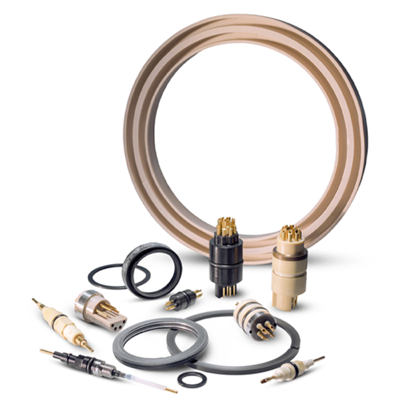
Check out our complete line of solutions for semiconductor manufacturing. From unique sealing designs and materials, such as Fusion® FKM and Chemraz® FFKM, to innovative chamber components using high-performance composites like our ONX®600 , Greene Tweed has an unmatched portfolio in the industry, a robust supply chain to enable market scale-up, and a broad global footprint.